
Young Researcher Paper Award 2025
🥇Winners
🥇Winners
Print: ISSN 0914-4935
Online: ISSN 2435-0869
Sensors and Materials
is an international peer-reviewed open access journal to provide a forum for researchers working in multidisciplinary fields of sensing technology.
Online: ISSN 2435-0869
Sensors and Materials
is an international peer-reviewed open access journal to provide a forum for researchers working in multidisciplinary fields of sensing technology.
Tweets by Journal_SandM
Sensors and Materials
is covered by Science Citation Index Expanded (Clarivate Analytics), Scopus (Elsevier), and other databases.
Instructions to authors
English 日本語
Instructions for manuscript preparation
English 日本語
Template
English
Publisher
MYU K.K.
Sensors and Materials
1-23-3-303 Sendagi,
Bunkyo-ku, Tokyo 113-0022, Japan
Tel: 81-3-3827-8549
Fax: 81-3-3827-8547
MYU Research, a scientific publisher, seeks a native English-speaking proofreader with a scientific background. B.Sc. or higher degree is desirable. In-office position; work hours negotiable. Call 03-3827-8549 for further information.

MYU Research
(proofreading and recording)

MYU K.K.
(translation service)
The Art of Writing Scientific Papers
(How to write scientific papers)
(Japanese Only)
is covered by Science Citation Index Expanded (Clarivate Analytics), Scopus (Elsevier), and other databases.
Instructions to authors
English 日本語
Instructions for manuscript preparation
English 日本語
Template
English
Publisher
MYU K.K.
Sensors and Materials
1-23-3-303 Sendagi,
Bunkyo-ku, Tokyo 113-0022, Japan
Tel: 81-3-3827-8549
Fax: 81-3-3827-8547
MYU Research, a scientific publisher, seeks a native English-speaking proofreader with a scientific background. B.Sc. or higher degree is desirable. In-office position; work hours negotiable. Call 03-3827-8549 for further information.
MYU Research
(proofreading and recording)
MYU K.K.
(translation service)
The Art of Writing Scientific Papers
(How to write scientific papers)
(Japanese Only)
Sensors and Materials, Volume 31, Number 8(2) (2019)
Copyright(C) MYU K.K.
Copyright(C) MYU K.K.
|
pp. 2511-2525
S&M1952 Research Paper of Special Issue https://doi.org/10.18494/SAM.2019.2443 Published: August 19, 2019 Experimental Comparison of Rapid Large-area Direct Electron Beam Exposure Methods with Plasmonic Devices [PDF] Akio Higo, Tomoki Sawamura, Makoto Fujiwara, Eric Lebrasseur, Ayako Mizushima, Etsuko Ota, and Yoshio Mita (Received May 23, 2019; Accepted July 25, 2019) Keywords: electron beam lithography, character projection, variable-shaped beam, nanopatterns, color filter
We have quantitatively investigated a periodic nanostructure exposure process by electron beam lithography (EBL). The targeted applications are nano- to micro-electromechanical systems (NEMS/MEMS), nanophotonics, surface plasmonic structures, and metamaterials. It is confirmed that the character projection (CP) method can obtain both high throughput and high resolution simultaneously as compared with the variable-shaped beam (VSB) method. We used square, triangular, and octagonal CP stencil masks to realize a nanohole array (NHA) of 10.4 mm2 area. The holes were placed in both square and hexagonal grid configurations. We measured the hole patterns by scanning electron microscopy (SEM) and scanning probe microscopy (SPM). Also, the effect of NHA size variation was measured on the basis of optical absorption spectra obtained using a system consisting of an optical microscope and a spectrum analyzer. The spectrum variation was confirmed to be in good agreement with the local size variation; identically fabricated NHAs showed identical spectra. It is therefore possible to control the nanometric critical dimensions by using NHAs as process indicators.
Corresponding author: Akio Higo and Yoshio Mita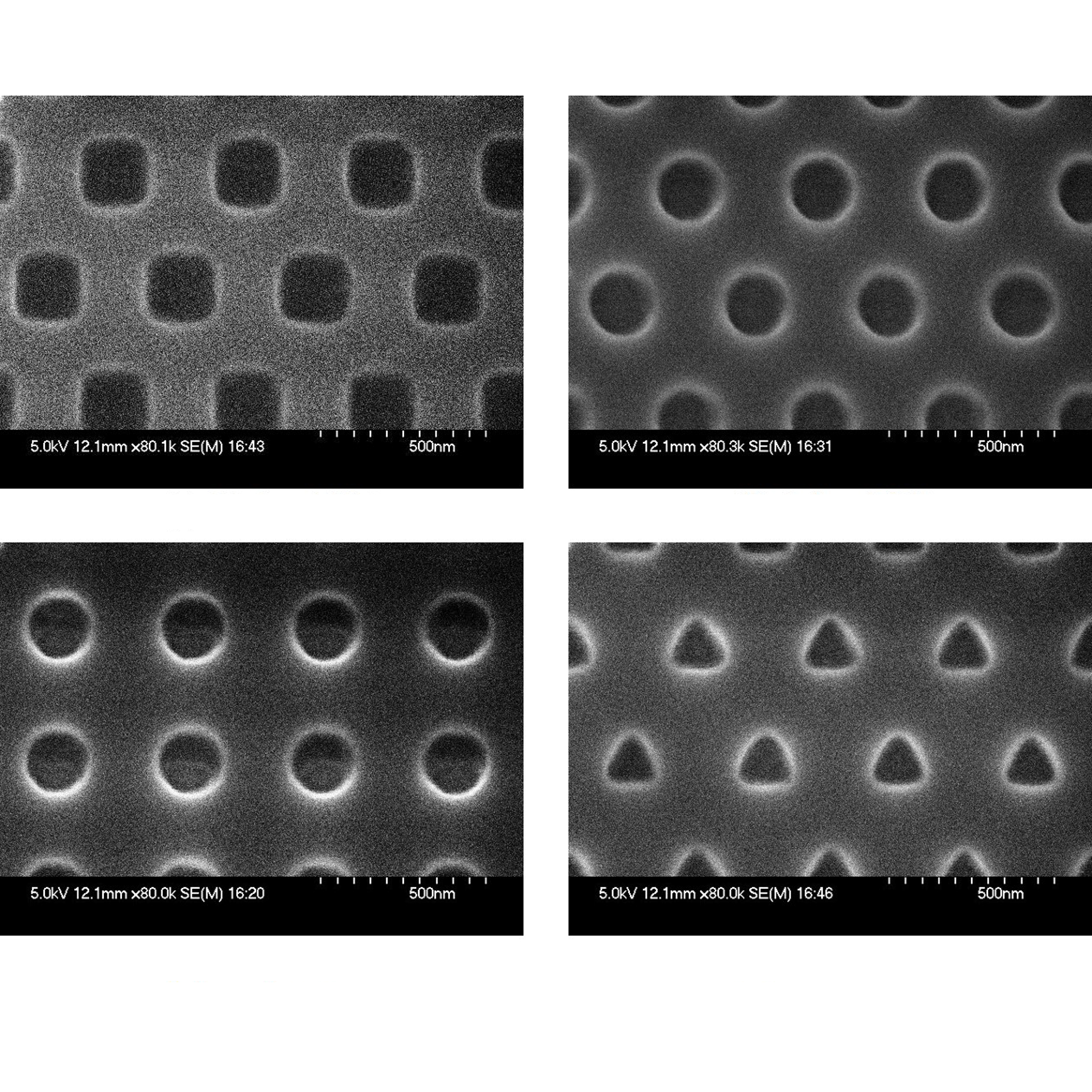  This work is licensed under a Creative Commons Attribution 4.0 International License. Cite this article Akio Higo, Tomoki Sawamura, Makoto Fujiwara, Eric Lebrasseur, Ayako Mizushima, Etsuko Ota, and Yoshio Mita, Experimental Comparison of Rapid Large-area Direct Electron Beam Exposure Methods with Plasmonic Devices, Sens. Mater., Vol. 31, No. 8, 2019, p. 2511-2525. |
Forthcoming Regular Issues
Forthcoming Special Issues
Special Issue on Signal Collection, Processing, and System Integration in Automation Applications 2026
Guest editor, Hsiung-Cheng Lin (National Chin-Yi University of Technology), Ming-Te Chen (National Chin-Yi University of Technology), and Chin-Yi Cheng (National Yunlin University of Science and Technology)
Call for paper
Special Issue on Advanced GeoAI for Smart Cities: Novel Data Modeling with Multi-source Sensor Data
Guest editor, Prof. Changfeng Jing (China University of Geosciences Beijing)
Call for paper
Special Issue on Advanced Sensor Application Development
Guest editor, Shih-Chen Shi (National Cheng Kung University) and Tao-Hsing Chen (National Kaohsiung University of Science and Technology)
Call for paper
Special Issue on Mobile Computing and Ubiquitous Networking for Smart Society
Guest editor, Akira Uchiyama (The University of Osaka) and Jaehoon Paul Jeong (Sungkyunkwan University)
Call for paper
Special Issue on Advanced Materials and Technologies for Sensor and Artificial- Intelligence-of-Things Applications (Selected Papers from ICASI 2026)
Guest editor, Sheng-Joue Young (National Yunlin University of Science and Technology)
Conference website
Call for paper
Special Issue on Biosensing Devices
Guest editor, Kiyotaka Sasagawa (Nara Institute of Science and Technology)
Call for paper
-
For more information of Special Issues (click here)
-
Special Issue on Innovations in Multimodal Sensing for Intelligent Devices, Systems, and Applications (submission closed)
- Accepted papers (click here)
- Implementation of Deep-Neural-Network–based Unmanned Aerial Vehicle Platform for Fire Smoke Response: Wildfire Smoke Description Experiments
Tae-Hwan Kim, Eun-Su Seo, and Se-Hyu Choi - User-centric Real-time System for Building Disaster Alerts
Tae-Hwan Kim, Eun-Su Seo, and Se-Hyu Choi
- Implementation of Deep-Neural-Network–based Unmanned Aerial Vehicle Platform for Fire Smoke Response: Wildfire Smoke Description Experiments
- Accepted papers (click here)
- High-precision Autonomous Driving Map Quality Inspection Indicator System and Evaluation Method
Chengcheng Li, Ming Dong, Hongli Li, Xunwen Yu, Yongxuan Liu, and Chong Zhang - Surface Albedo in Different Land Cover Types in Northeast China
Tao Pan, Fu Li, Yucheng Tao, Lijuan Zhang, and Xiaoyan Jiang
- High-precision Autonomous Driving Map Quality Inspection Indicator System and Evaluation Method
- Accepted papers (click here)
- Voltage Reflex and Equalization Charger for Series-connected Batteries
Cheng-Tao Tsai and Jia-Wei Lin
- Voltage Reflex and Equalization Charger for Series-connected Batteries
- Accepted papers (click here)
- Design and Development of a Fuzzy-logic-based Long-range Aquaculture System
Sheng-Tao Chen and Tai-I Chou
- Design and Development of a Fuzzy-logic-based Long-range Aquaculture System
Guest editor, Jiahui Yu (Research scientist, Zhejiang University), Kairu Li (Professor, Shenyang University of Technology), Yinfeng Fang (Professor, Hangzhou Dianzi University), Chin Wei Hong (Professor, Tokyo Metropolitan University), Zhiqiang Zhang (Professor, University of Leeds)
Call for paper
Special Issue on Novel Sensors, Materials, and Related Technologies on Artificial Intelligence of Things Applications
Guest editor, Teen-Hang Meen (National Formosa University), Wenbing Zhao (Cleveland State University), and Cheng-Fu Yang (National University of Kaohsiung)
Call for paper
Special Issue on Low-altitude Economy: Technologies, Infrastructure, and Applications
Guest editor, He Huang and Junxing Yang (Beijing University of Civil Engineering and Architecture)
Call for paper
Special Issue on Multisource Sensors for Geographic Spatiotemporal Analysis and Social Sensing Technology Part 5
Guest editor, Prof. Bogang Yang (Beijing Institute of Surveying and Mapping) and Prof. Xiang Lei Liu (Beijing University of Civil Engineering and Architecture)
Special Issue on Materials, Devices, Circuits, and Analytical Methods for Various Sensors (Selected Papers from ICSEVEN 2025)
Guest editor, Chien-Jung Huang (National University of Kaohsiung), Mu-Chun Wang (Minghsin University of Science and Technology), Shih-Hung Lin (Chung Shan Medical University), Ja-Hao Chen (Feng Chia University)
Conference website
Call for paper
Special Issue on Advances in Sensors and Computational Intelligence for Industrial Applications
Guest editor, Chih-Hsien Hsia (National Ilan University)
Call for paper
Special Issue on AI-driven Sustainable Sensor Materials, Processes, and Circular Economy Applications
Guest editor, Shih-Chen Shi (National Cheng Kung University) and Tao-Hsing Chen (National Kaohsiung University of Science and Technology)
Call for paper
Special Issue on Intelligent Sensing and AI-driven Optimization for Sustainable Smart Manufacturing
Guest editor, Cheng-Chi Wang (National Sun Yat-sen University)
Call for paper
- Accepted papers (click here)
Copyright(C) MYU K.K. All Rights Reserved.