
Young Researcher Paper Award 2025
🥇Winners
🥇Winners
Print: ISSN 0914-4935
Online: ISSN 2435-0869
Sensors and Materials
is an international peer-reviewed open access journal to provide a forum for researchers working in multidisciplinary fields of sensing technology.
Online: ISSN 2435-0869
Sensors and Materials
is an international peer-reviewed open access journal to provide a forum for researchers working in multidisciplinary fields of sensing technology.
Tweets by Journal_SandM
Sensors and Materials
is covered by Science Citation Index Expanded (Clarivate Analytics), Scopus (Elsevier), and other databases.
Instructions to authors
English 日本語
Instructions for manuscript preparation
English 日本語
Template
English
Publisher
MYU K.K.
Sensors and Materials
1-23-3-303 Sendagi,
Bunkyo-ku, Tokyo 113-0022, Japan
Tel: 81-3-3827-8549
Fax: 81-3-3827-8547
MYU Research, a scientific publisher, seeks a native English-speaking proofreader with a scientific background. B.Sc. or higher degree is desirable. In-office position; work hours negotiable. Call 03-3827-8549 for further information.

MYU Research
(proofreading and recording)

MYU K.K.
(translation service)
The Art of Writing Scientific Papers
(How to write scientific papers)
(Japanese Only)
is covered by Science Citation Index Expanded (Clarivate Analytics), Scopus (Elsevier), and other databases.
Instructions to authors
English 日本語
Instructions for manuscript preparation
English 日本語
Template
English
Publisher
MYU K.K.
Sensors and Materials
1-23-3-303 Sendagi,
Bunkyo-ku, Tokyo 113-0022, Japan
Tel: 81-3-3827-8549
Fax: 81-3-3827-8547
MYU Research, a scientific publisher, seeks a native English-speaking proofreader with a scientific background. B.Sc. or higher degree is desirable. In-office position; work hours negotiable. Call 03-3827-8549 for further information.
MYU Research
(proofreading and recording)
MYU K.K.
(translation service)
The Art of Writing Scientific Papers
(How to write scientific papers)
(Japanese Only)
Sensors and Materials, Volume 37, Number 3(2) (2025)
Copyright(C) MYU K.K.
Copyright(C) MYU K.K.
|
pp. 977-985
S&M3970 Research Paper https://doi.org/10.18494/SAM5547 Published: March 14, 2025 Sub-micrometer-sized Patterning of Photoresist by Electron Beam Projection Lithography Using Tabletop Scanning Electron Microscopy System and Stencil Masks [PDF] Mina Sato, Mie Tohnishi, Miho Fujimoto, and Akihiro Matsutani (Received January 15, 2025; Accepted March 5, 2025) Keywords: EPL, stencil masks, tabletop SEM, lithography, Si
We demonstrated a lithography technique using stencil masks and a tabletop scanning electron microscopy (SEM) system by applying electron beam projection lithography (EPL) technology. Si and Pt were used as stencil mask materials. Si has excellent fabrication workability, and Pt has excellent electron shielding. The lithography was performed at an incident electron energy of 5 to 10 kV, which is typically used in the tabletop SEM system. This technique achieves high throughput and can expose large areas at once. Sub-micrometer- and micrometer-sized patterns can be formed simultaneously.
Corresponding author: Mina Sato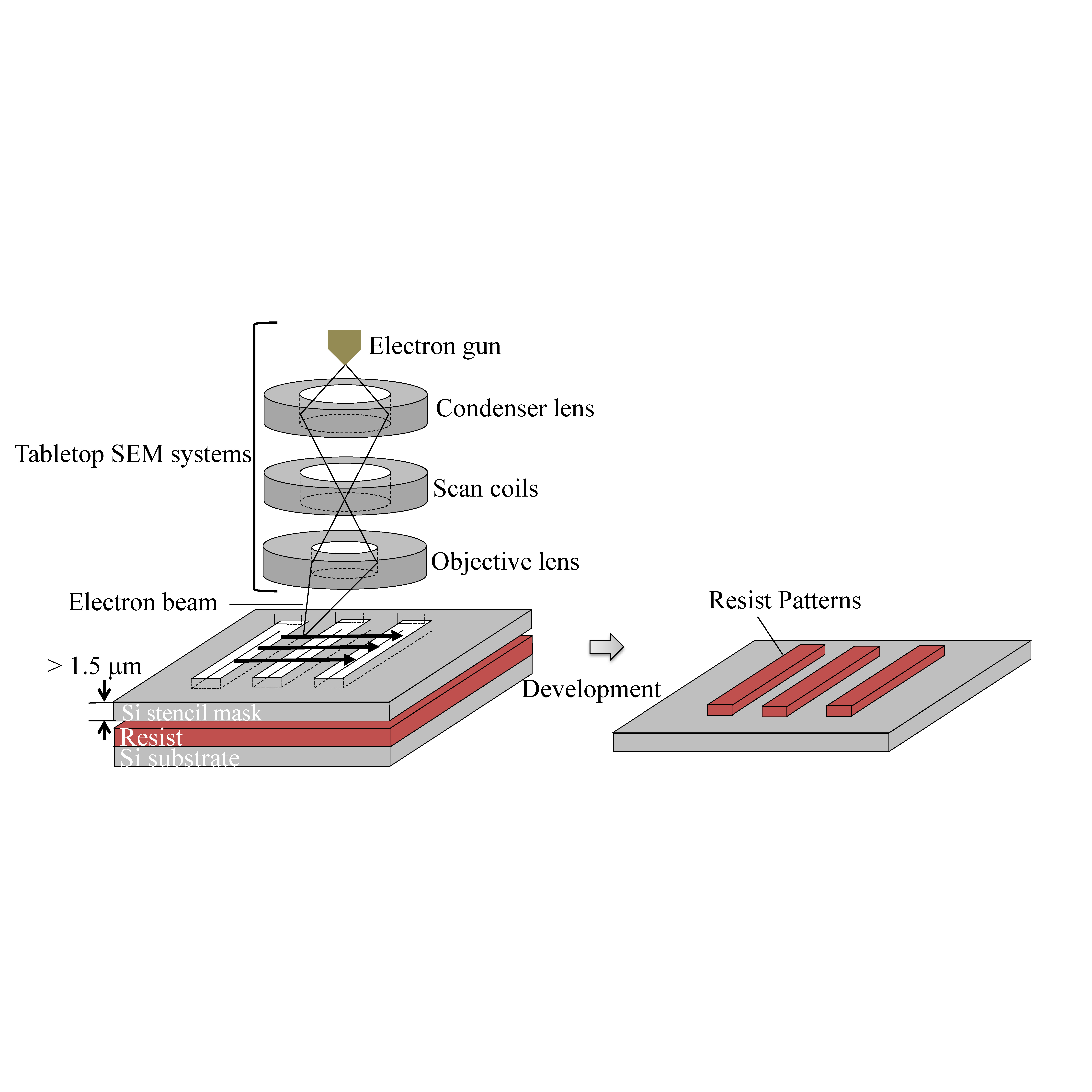  This work is licensed under a Creative Commons Attribution 4.0 International License. Cite this article Mina Sato, Mie Tohnishi, Miho Fujimoto, and Akihiro Matsutani, Sub-micrometer-sized Patterning of Photoresist by Electron Beam Projection Lithography Using Tabletop Scanning Electron Microscopy System and Stencil Masks, Sens. Mater., Vol. 37, No. 3, 2025, p. 977-985. |
Forthcoming Regular Issues
Forthcoming Special Issues
Special Issue on Signal Collection, Processing, and System Integration in Automation Applications 2026
Guest editor, Hsiung-Cheng Lin (National Chin-Yi University of Technology), Ming-Te Chen (National Chin-Yi University of Technology), and Chin-Yi Cheng (National Yunlin University of Science and Technology)
Call for paper
Special Issue on Advanced Sensor Application Development
Guest editor, Shih-Chen Shi (National Cheng Kung University) and Tao-Hsing Chen (National Kaohsiung University of Science and Technology)
Call for paper
Special Issue on Sensing Beyond Transduction: Materials, Devices, and Signal Processing for Intelligent Sensory Systems
Guest editor, Masayuki Sohgawa (Niigata University)
Call for paper
Special Issue on Advanced Materials and Technologies for Sensor and Artificial- Intelligence-of-Things Applications (Selected Papers from ICASI 2026)
Guest editor, Sheng-Joue Young (National Yunlin University of Science and Technology)
Conference website
Call for paper
Special Issue on Biosensing Devices
Guest editor, Kiyotaka Sasagawa (Nara Institute of Science and Technology)
Call for paper
Special Issue on Mobile Computing and Ubiquitous Networking for Smart Society
Guest editor, Akira Uchiyama (The University of Osaka) and Jaehoon Paul Jeong (Sungkyunkwan University)
Call for paper
-
For more information of Special Issues (click here)
-
Special Issue on Novel Sensors, Materials, and Related Technologies on Artificial Intelligence of Things Applications
- Accepted papers (click here)
- Negative Temperature Coefficient Thermistor with Multilayer Thin-film Structure AlN/VOx/AlN on Si(100) Substrate
Chen-Hung Yen, Ing-Jiunn Su, and Hui-Huang Hsieh
- Negative Temperature Coefficient Thermistor with Multilayer Thin-film Structure AlN/VOx/AlN on Si(100) Substrate
- Accepted papers (click here)
- Design and Development of a Fuzzy-logic-based Long-range Aquaculture System
Sheng-Tao Chen and Tai-I Chou - Payload Measurement of Heavy Vehicles by Measuring Deflection of Leaf Springs for Use of IoT
Shan-Kuo Yang and Kai-Jung Chen
- Design and Development of a Fuzzy-logic-based Long-range Aquaculture System
Guest editor, Teen-Hang Meen (National Formosa University), Wenbing Zhao (Cleveland State University), and Cheng-Fu Yang (National University of Kaohsiung)
Call for paper
Special Issue on Low-altitude Economy: Technologies, Infrastructure, and Applications
Guest editor, He Huang and Junxing Yang (Beijing University of Civil Engineering and Architecture)
Call for paper
Special Issue on Materials, Devices, Circuits, and Analytical Methods for Various Sensors (Selected Papers from ICSEVEN 2026)
Guest editor, Chien-Jung Huang (National University of Kaohsiung), Mu-Chun Wang (Minghsin University of Science and Technology), Shih-Hung Lin (Chung Shan Medical University), Ja-Hao Chen (Feng Chia University)
Conference website
Call for paper
Special Issue on Sensing and Data Analysis Technologies for Living Environment, Health Care, Production Management, and Engineering/Science Education Applications (2026)
Guest editor, Chien-Jung Huang (National University of Kaohsiung), Rey-Chue Hwang (I-Shou University), Ja-Hao Chen (Feng Chia University), Ba-Son Nguyen (University of Economics Ho Chi Minh City)
Call for paper
Special Issue on Multisource Sensors for Resource and Environmental Monitoring: Theories, Models, Methods, and Application
Guest editor, Chao Chen (Suzhou University of Science and Technology)
Call for paper
Special Issue on Spatial Intelligence, Digital Twins, and AI-driven Smart Systems for Next-Generation Built Environment
Guest editor, Jaekang Lee (Dong-A University), Myeong Hun Jeong (Chosun University), and Dong Ha Lee (Kangwon National University),
Call for paper
Special Issue on Advances in Sensors and Computational Intelligence for Industrial Applications: Part 2 (submission closed)
Guest editor, Chih-Hsien Hsia (National Ilan University)
Call for paper
Special Issue on Intelligent Sensing and AI-driven Optimization for Sustainable Smart Manufacturing
Guest editor, Cheng-Chi Wang (National Sun Yat-sen University)
Call for paper
- Accepted papers (click here)
Copyright(C) MYU K.K. All Rights Reserved.